A TTL CPU I built a long time ago when I bought a huge stock of NOS TTL chips on ebay
Details#
4 Bit TTL CPU#
A few years ago I purchased a large quantity of old LS-TTL chips in an internet auction. Wanting to put them to use, I started to design a CPU around them.
I decided to go with a 4 bit datapath to reduce the circuit size. The CPU uses separated program and data memory, a Harvard architecture. The width of the program memory is 8-bit. A side effect is, that there is no way to write to the program memory. This forbids self-modifying code and renders constructs like subroutines very difficult. The data memory consists of 32 4-bit “registers”. All operations are performed on a single accumulator. Actually, the general idea behind the architecture can be very well compared to the Microchip PIC. See below for an instruction reference.
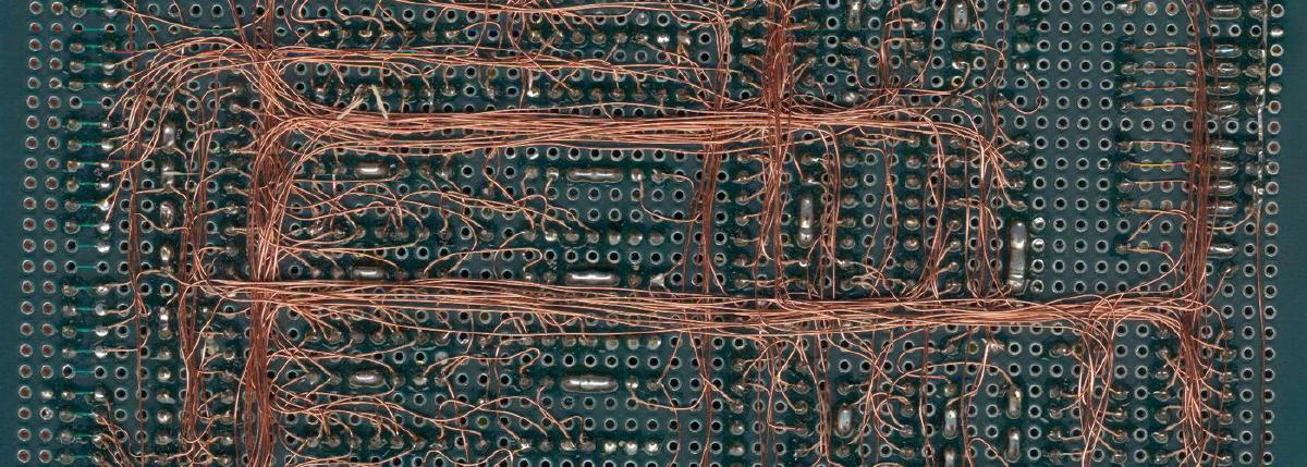
The CPU circuit was designed on paper and built on three veroboards. It is difficult to believe, but the circuit worked on the first power up. A few photos of this mess are displayed at the bottom of this page.
Registers#
| Register | Bits | Description |
|---|---|---|
| PC | 11:0 | Program counter |
| Accu | 3:0 | Accumulator |
| r00-r15 | 3:0 | 16 Work registers |
| r16-r23 | 3:0 | 8 I/O registers |
| r24-r31 | 3:0 | Scratchpad |
| Flags:C | - | Carry/Borrow |
| Flags:Z | - | Zero flag |
Instruction list#
| Symbol | Meaning |
|---|---|
| r | register |
| i | immediate value |
| a | address |
| Ac | Accumulator |
| r16 | [r0..r15] |
| r32 | [r0..r32] |
| imm4 | [0 .. 15] |
| add12 | [0 .. 4095] |
| Mnemonic | Machine code | Length | Cycles | Flags | Operation |
|---|---|---|---|---|---|
| ADC r16 | 0011 rrrr | 1 | 1 | ZC | Ac=Ac+r16+C |
| ADC #imm4 | 0111 iiii | 1 | 1 | ZC | Ac=Ac+imm4+C |
| OR r16 | 0001 rrrr | 1 | 1 | Z- | Ac=Ac OR r16 |
| AND r16 | 0000 rrrr | 1 | 1 | Z- | Ac=Ac AND r16 |
| XOR r16 | 0010 rrrr | 1 | 1 | Z- | Ac=Ac XOR r16 |
| XOR #imm4 | 0110 iiii | 1 | 1 | Z- | Ac=Ac XOR imm4 |
| LDI #imm4 | 0100 iiii | 1 | 1 | Z- | Ac=imm4 |
| STA r32 | 110r rrrr | 1 | 1 | – | r32=Ac |
| LDA r32 | 111r rrrr | 1 | 1 | Z- | Ax=r32 |
| SEC | 0101 1000 | 1 | 1 | -C | C=1 |
| CLC | 0101 0000 | 1 | 1 | -C | C=0 |
| ROL | 0101 1100 | 1 | 1 | ZC | Ac=(Ac«1)+Cold, Cnew=Accu Bit 3 |
| LSL | 0101 0100 | 1 | 1 | ZC | Ac=Ac«1, Cnew=Accu Bit 3 |
| NOP | 0110 0000 | 1 | 1 | – | does nothing. (in fact it executes Ac=Ac XOR 00) |
| JCS $add12 | 1000 aaaa aaaa aaaa | 2 | 2 | – | Jump if C=1 |
| JCC $add12 | 1001 aaaa aaaa aaaa | 2 | 2 | – | Jump if C=0 |
| JMP $add12 | 1010 aaaa aaaa aaaa | 2 | 2 | – | Jump always |
| JNZ $add12 | 1011 aaaa aaaa aaaa | 2 | 2 | – | Jump if Z=0 |
Images#
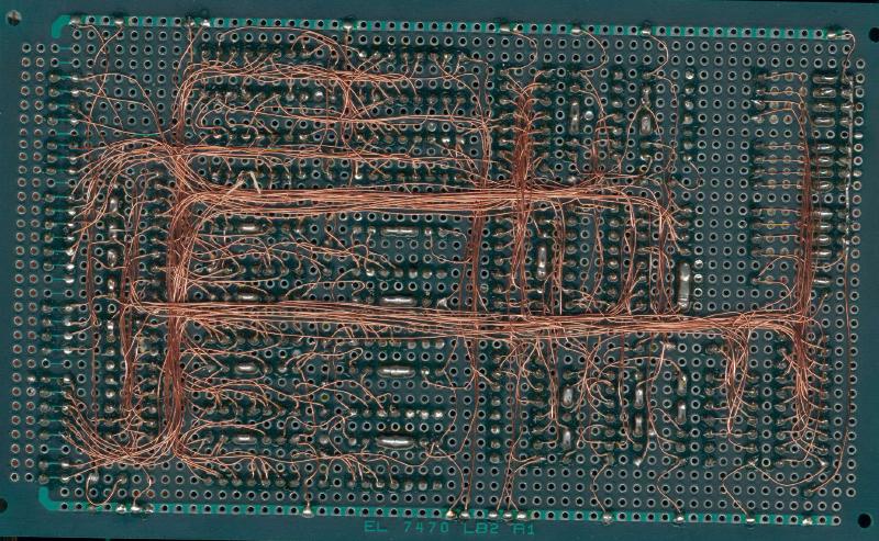
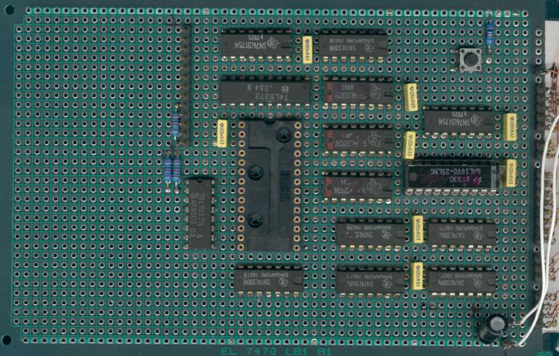
ALU-Board component and solder side. This boards holds the ALU, registerfile, accumulator, flags and some bus muxes. The ALU consists of a 4 bit boolean function unit (8x LS00 to the right), a 4 bit adder (LS283), 4 bit XOR (LS86) and the result multiplexer/shifter (2x LS153). The registerfile is a simple single port 256x4 sram (Harris 6561). The two LS175 hold the accumulator and the flags. The black components to the left contain various status LEDs.
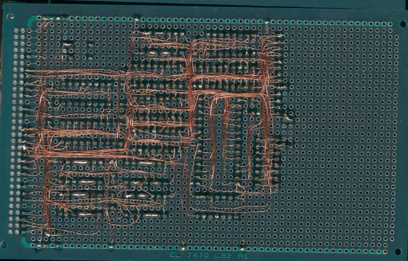
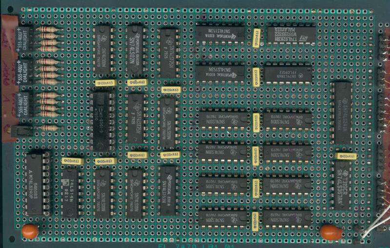
Program/Control component and solder side. Holds the program ROM, the program counter logic and various instruction decoding. The program counter logic consists of the PC (3x LS193), branch logic (LS 175 and more ?) and a branch adress register (LS373,LS175). The GAL and 4x LS00 are used as instruction decoder. The GAL replaces around 8-10 ICs of random logic, so it is really put to good use.
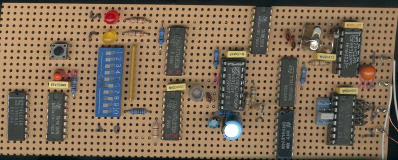
PLL board, component side. This board generates the required two phase clock signal. In addition it allows single step clocking for debug purposes. The clock frequency can be adjusted between fractions and multiples of a MHz, using the DIP switches and the jumpers. The two phase clock and lots of extra trouble could probably have been avoided by spending additional thought on the design.
(c) 2002 Tim - Last change: 16 October 2002
Exported from Hackaday.io 4 Bit TTL CPU